In the previous post on CMOS inverter, we have seen in detail the working of a CMOS inverter circuit. We are also now familiar with the typical voltage transfer characteristics of a CMOS inverter. Finally, we have seen the calculations for a very important parameter of an inverter called noise margins. We are also familiar with the physical meaning of these noise margins.
In this post, we will continue forward with our study on the CMOS inverter with new parameters that one should always keep in mind while designing digital CMOS circuits. Recall that in the previous post, we discussed the noise margins as an important parameter from the digital design point of view. This noise margins defined the allowable discrepancy we can have in the input of the inverter. This was mainly focussed on the noise considerations of a digital circuit. In this post, we will focus on the parameters that define the speed of operation of a CMOS circuit.
Before we begin, the reader should be comfortable with the mathematical derivations that we have done in the previous chapter on CMOS inverter. Also, the typical voltage transfer characteristics should be very familiar by now. In the sections that follow, we will first define the propagation delay in a generic manner. Then, we will understand the propagation delay for CMOS inverters. Finally, we will see what causes these delays and what we can do to minimize them.
Defining “Delay” in a circuit
Every circuit has some parasitic capacitance components associated with it. In the chapter for non-ideal effects in MOSFETs, we have discussed the parasitic capacitance present in the MOSFET device. These capacitance results in delaying the voltage change in the circuit. So we will get limitations in our speed of operation depending on how fast we can charge or discharge these capacitors.
To illustrate how the capacitances affect the output waveforms, we take some examples of waveforms. We will also define certain quantities such as “Propagation Delay” and “Transition Delay,” which will help us in quantifying the speed performance of our inverter.
Propagation delay

Suppose that we have a CMOS inverter whose output is connected to some next stage circuits. To test the speed performance of our circuit, we apply a step voltage at the input, as shown in the schematic in figure 1. Note that in the schematic, we have represented the capacitance offered by the next stage by a load capacitance 

In the plot of output voltage in figure 2, there are two time intervals marked by 


The propagation delay for high to low is given by 

The propagation delay 

Transition time
We consider a similar situation for defining another similar quantity called transition time. For this, we also consider a step input voltage, the corresponding output curve obtained is shown in figure 3.

In the plot of the output voltage, there are two time intervals marked as 


In a similar manner the transition time is defined by taking the average of these two quantities:

Practical input signals
The input signals to our CMOS inverter in the previous discussions was taken as an exact step function. But, for practical scenarios the inverter will also be driven by the output signal of some other logic gate. This means that the input signal to the inverter we are studying will be more of a “ramp-signal” rather than a step signal. To illustrate the effect of such an input signal, we have plotted the input and output voltage curves in figure 4.

Observe from the figure that the output signal starts to climb up once when the input signal goes below the point 
“Rise-time” and “Fall-time”
In this section, we will derive the mathematical expressions for the propagation delay 
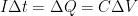
- The change in charge across a capacitor is given by the current flowing through it times the time interval over which we see the change in charge. This quantity is also equal to the capacitance times the change in voltage across the capacitor. Mathematically:
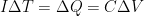
 . But, if we want to obtain insights on the working of a capacitive circuit using this formula, then we will use the average current “<I>” instead of the instantaneous current “I” in the equation. For many cases, we will be able to deduce the dependence of delay on different parameters by solving this equation only.
- For a capacitor with an initial voltage across it as
and if we know that the final steady-state value of the voltage across it is
. We can write the voltage across the capacitance as a function of time to be:
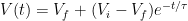
Here the quantity 

Approximate Calculation
In this section, we will do an approximate calculation to figure out the propagation delay of an CMOS inverter if we have a capacitive load
When we cross the rising edge, then the input to the circuit is 

At the instant of switching, the drain-to-source voltage of NMOS is equal to 
![I_{dn} = \frac{k_{n}}{2} [(V_{dd} - V_{Tn})^2]](https://s0.wp.com/latex.php?latex=+I_%7Bdn%7D+%3D+%5Cfrac%7Bk_%7Bn%7D%7D%7B2%7D+%5B%28V_%7Bdd%7D+-+V_%7BTn%7D%29%5E2%5D&bg=ffffff&fg=000&s=0&c=20201002)
Then, as the load capacitor 
Our propagation delay is defined by the time in which output falls from 


![I_{dn} = \frac{k_{n}}{2} [2(V_{dd} - V_{Tn})(V_{dd}/2) - (V_{dd}/2)^{2}]](https://s0.wp.com/latex.php?latex=+I_%7Bdn%7D+%3D+%5Cfrac%7Bk_%7Bn%7D%7D%7B2%7D+%5B2%28V_%7Bdd%7D+-+V_%7BTn%7D%29%28V_%7Bdd%7D%2F2%29+-+%28V_%7Bdd%7D%2F2%29%5E%7B2%7D%5D&bg=ffffff&fg=000&s=0&c=20201002)
Taking these two extreme values of the current, we calculate the average current as:
![I_{avg} = \frac{k_{n}}{4}[(7/4)V_{dd}^{2} - 3 V_{dd} V_{Tn} + V_{Tn}^{2}]](https://s0.wp.com/latex.php?latex=+I_%7Bavg%7D+%3D+%5Cfrac%7Bk_%7Bn%7D%7D%7B4%7D%5B%287%2F4%29V_%7Bdd%7D%5E%7B2%7D+-+3+V_%7Bdd%7D+V_%7BTn%7D+%2B+V_%7BTn%7D%5E%7B2%7D%5D+&bg=ffffff&fg=000&s=0&c=20201002)
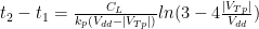
We, will put this into the equation:

Here, 

Simplifying the above equations and solving for

Here, 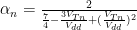
Similarly, the results for 

The value obtained for propagation delay for low to high transition is given by:

Here, 


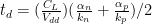
Therefore, the propagation delay of the circuit is given by the average:
Inference from approximate calculation
- The propagation delays are inversely proportional to the
and
values. This means as the conductivity of the transistors in there “on-state” increase, the delay time decrease. This also makes sense intuitively, as the series resistance in the RC circuit decreases, the time constant also decreases. Thus, there is faster rate of charging and discharging.
- The value of
depends on the value of the threshold voltage and supply voltage. Consider that the
. If, we want to match the delay values for high-to-low and low-to-high transitions, then:

If we have 
- The delay time is directly proportional to the load capacitance
. From a design point of view, the parasitic capacitances present in the CMOS inverter should be aimed to be kept at a minimum value.
- The delay time is inversely proportional to the supply voltage
. Considering that the
Accurate calculations
In this section, we will derive a much more accurate value for the delay time. We will only go over the calculations for the output transition from low level to high level. For this purpose we will consider two time intervals. From 

We consider that the PMOS transistor stays in it’s saturation region for a relatively very short time 
![I_{dp} = \frac{k_{p}}{2} [(V_{dd} - \mid V_{Tp}) \mid)^2]](https://s0.wp.com/latex.php?latex=+I_%7Bdp%7D+%3D+%5Cfrac%7Bk_%7Bp%7D%7D%7B2%7D+%5B%28V_%7Bdd%7D+-+%5Cmid+V_%7BTp%7D%29+%5Cmid%29%5E2%5D&bg=ffffff&fg=000&s=0&c=20201002)
We put this value of the current in the equation:
Here, 

Simplifying the equations and solving for

Then, we will solve for the time 
![I_{dp} = (k_{p}/2) [2(V_{dd} - \mid V_{Tp} \mid)(V_{dd} - V_{out}) - (V_{dd} - V_{out})^{2}]](https://s0.wp.com/latex.php?latex=+I_%7Bdp%7D+%3D+%28k_%7Bp%7D%2F2%29%C2%A0%5B2%28V_%7Bdd%7D+-+%5Cmid+V_%7BTp%7D+%5Cmid%29%28V_%7Bdd%7D+-+V_%7Bout%7D%29+-+%28V_%7Bdd%7D+-+V_%7Bout%7D%29%5E%7B2%7D%5D+&bg=ffffff&fg=000&s=0&c=20201002)
We put the value of 

This gives us an differential equation which can be solved to find 

Suppose that 

RHS = 
Solve the above equations for “t” running from 

Simplifying, we get:
Here, 


Finally, we get:

suppose that 

The rise in output voltage when we apply a negative edge input is shown in figure 7. For 


The derivation for

The fall in output voltage on the application of a rising edge input signal is shown in figure 8. Similar to the charging of capacitance, the discharging is also divided into two regions. For 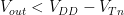


The readers are advised to check that the inference is drawn in the case of approximate calculation also holds for the accurate calculations. Note that the “on-resistance” is inversely proportional to the
If we plot the above delay values w.r.t. the threshold voltages, we observe that the propagation delays increase with the rise in the magnitude of threshold voltages. Therefore having low threshold voltage values improves the speed of operation of the circuit.
Note that the hand calculations done in this section are not exact. They don’t take into account the non-ideal effects of the MOSFETs. For the exact relationships, one should use the different circuit simulators available. But, the hand calculations do provide a good amount of design insights. We must only proceed with simulations when we have some quantitative idea about the output of the circuit.
Factors affecting propagation delay in CMOS inverters
We have earlier discussed the dependence of the propagation delay on various factors. In this section, we will summarise them and also look over some of the consequences from a design point of view.
Threshold Voltage
With the decrease in the value of threshold voltage, the propagation delay also decreases. Thus, for faster circuit operation, we would like to choose MOSFETs with very low threshold voltages. This is why we have seen that the body and source terminals are connected in both the NMOS and PMOS in order to remove the body effect.
Width (W) of the MOSFETS
As we have seen that the propagation delay decreases as we increase the
But, this increase in width also results in an increase of the parasitic capacitance in the CMOS inverter. If this inverter is driving some next stage logic gate, then it will see a high capacitive load. This will ultimately result in the degradation in the speed of the overall circuit.
Supply voltage
The propagation delay has an inverse relation with the supply voltage(
But, for small devices, there is an upper limit to the supply voltage that can be used in order to not damage the circuit. Also, an increase in supply voltage results in the dynamic power consumption to increase.
Capacitive load
The parasitic capacitance present in the overall CMOS inverter circuit manifests as the capacitive load(
Short channel effects
As we have seen in the previous that there are a lot of non-ideal effects in the MOSFET device. But, we have done all our calculations only considering ideal IV characteristics. One of the most important effects of propagation delay considerations is “velocity saturation.”
We are now aware that channel length is kept minimum in order to increase the conductivity of the device. But, for short channel device, the saturation happens due to velocity saturation and not due to channel length modulation. Thus, the saturation current will be lower than that in long channel devices. Therefore, the propagation delay will be more.
Maximum operating frequency
Supposed that after optimizing the values of the MOSFETs in the CMOS inverter, we achieve a minimum delay of 

But, we generally operate our digital circuit around the range 
We have a lot of logic gates cascaded together, and each of these logic gates uses multiple CMOS inverters. Therefore the cumulative delay of the whole circuit is much more than 
The capacitance of CMOS inverters
Till now, we have been representing the capacitive load offered by the next stage with a simple capacitive load (
It should be clear by now that the capacitive load is just a manifestation of the parasitic capacitance in the MOSFETs and the capacitive elements present in the wiring used to connect the devices together. The different capacitance that constitutes our final

We consider a circuit of two CMOS inverters. There are a total of four transistors in the circuit, namely M1, M2, M3, M4. In the circuit schematic, the capacitive components shown are due to gate-to-drain capacitance (


The circuit shown in the figure is quite complex to be solved by hand. Thus, we will make some modifications to the model in order to get a simpler circuit. The load capacitance value that will be obtained from this simplified model will not be accurate but will still give us enough insights. One thing to note that the wiring capacitance that we have mentioned becomes an important parameter as we scale down our ICs.
The capacitors

So, we shift the gate-to-drain capacitance in the circuit and place them in parallel with 
Thus, our final expression for the load capacitance becomes:

Conclusion
In this chapter, we have seen how the speed performance of a CMOS inverter is quantified. We derived the formulae that define the propagation delay in a CMOS inverter circuit. We also saw how different parameters in the circuit affect the propagation delay of a CMOS inverter. Keep in mind that the CMOS inverter forms the building blocks for different types of logic gates. Hence, the delay in an overall logic circuit will also depend upon the delay caused by the CMOS inverters used.
One of the points we mentioned earlier that the speed of operation increases with an increase in supply voltage. But, also an increase in supply voltage value will result in more dynamic power dissipation in the circuit. We haven’t discussed why this is the case. The next post in this CMOS course is aimed at understanding this kind of effects only. We will learn about the different types of power consumption in a CMOS inverter and the factors that influence it.
