Microprocessors and microcontrollers are primarily used to process data. However, their applications are myriad only when they are interacting with the outside world.
And they do that via an assortment of input and output devices. It is impossible to name a real-life application of an SoC where I/O devices are not involved. There are either displays, sensors, actuators, keyboards, or other devices that are connected to a microprocessor.
We know that a processor has a finite number of pins that it can use to interface with external devices. What happens in the case of having more I/O devices than pins? That’s where Programmable Peripheral Interface chips come into the picture.
In this post, we will be taking a look at one of the most popular PPI chips, the 8255 from Intel. This is our ultimate guide on everything related to the 8255.
Note
‘Peripherals’ is another name for ‘i/o devices.’ So, don’t get confused.
Contents
What is the use of 8255 IC?
The 8255 is a programmable chip used for interfacing peripheral devices. It connects with a processor or a controller and increases the number of I/O pins that can be used in the system. It has three 8-bit ports used to connect I/O devices.
Pause. What does that mean?
That means we have 24-pins for interfacing I/O devices that are divided into three ports. Why? For additional control and features. We’ll find out more about that in the subsequent sections.
Features of 8255 Programmable Peripheral Interface
Important features of the 8255 are listed below:
- 8255 is a Programmable Peripheral Interface, available in the form of a 40 pin IC which works on a power supply of +5 V DC.
- It is compatible with a wide range of microprocessors and microcontrollers, making it widely popular.
- It has three 8-bit I/O: Ports A, B, and C.
- Port A and port B can function as 8-bit input or output ports.
- Bits of port C are divided into two subgroups of 4 bits each – port C upper and port C lower.
- There are other control pins which are used to specify and control the flow of data and operation of the 8255. We’ll check them out soon.
- The port pins have the ability to source 1 mA current at 1.5 V when programmed to function as output pins. This provides the capability of driving Darlington transistors for applications such as printers and high voltage displays.
- The most important feature of 8255 is that it is ‘programmable.’ This means that the operation of 8255 can be controlled by programming the microprocessor appropriately. This gives us the freedom to use 8255 in a number of ways without having to change the wiring and connections.
- It has a few different modes of operation. This is awesome because we get the freedom to choose from a bunch of different functionalities.
Let us understand the pin diagram and function of each pin of 8255. Then, we will learn the functioning of 8255 and different modes of operations in detail.
Pin diagram of 8255

| Pin name | Number of pins | Description |
| Vcc | 1 | Used to supply power to the IC. Usually at +5 V dc with respect to ground. |
| Ground | 1 | Ground pin. All the voltages (signals) are measured with respect to this pin. It is connected to the common ground of the circuit. |
| PA0-PA7 | 8 | These 8-bit bi-directional I/O pins are used to send data to output from a device and to receive data from an input device. |
| PB0-PB-7 | 8 | These 8-bit bi-directional I/O pins are used to send data to an output device and to receive data from an input device. |
| PC0-PC3 | 4 | These four pins are used by 8255 for communicating with an I/O device. |
| PC4-PC7 | 4 | These four pins are used by 8255 for communicating with an I/O device. |
| D0-D7 | 8 | These are the data pins used by the Master (uP/uC) to communicate with 8255. All the data to be transmitted and received and control instructions are transmitted to and from 8255 through these pins. These are connected to the data bus of the microprocessor. |
| CS | 1 | This is an active low input pin. The microprocessor uses this input to select the chip 8255. In other words, the microprocessor uses this pin to say to 8255 that “Hey!! Now I am talking to you. And I will keep talking to you until this CS signal remains low.” |
| RD | 1 | This is also an active low input pin used by the microprocessor to tell 8255 that it wants to read data from one of its ports. |
| WR | 1 | This is also an active low input pin used by the microprocessor to tell 8255 that it wants to write data to one of its ports. |
| A1, A0 | 2 | These are the port address pins. They are used to select the port with which the microprocessor intends to communicate. For values of A1A0:
00 = Port A is selected 01 = Port B is selected 10 = Port C is selected 11 = Control port is selected. |
| Reset | 1 | An active high input. Used to reset 8255. Immediately after reset, all the three ports work as input ports in mode 0. |
Block diagram and internal structure of 8255

Let’s break down the functionality of each block.
- Data bus buffer: It is a bidirectional (tri-state) data bus. Notice that this connects every single block in 8255 with each other except the read-write control logic block. All the data flows through this bus.
- Ports A, B, and C are divided into two groups.
- Group A: Port A (PA0-PA7) + Port C upper (PC4-PC7)
- Group B: Port B (PB0-PB7) + Port C upper (PC0-PC3)
- There are separate control units for Group A and Group B that get their control signals from the main read-write logic control logic block. The control logic receives individual control signals as inputs and responds accordingly.
- Group A control and Group B control blocks are connected to their respective Group blocks. They control the flow of data and modes of operation at those ports.
- Controls of group A and group B, represented by the control blocks ‘group A control‘ and ‘group B control‘ together make up ‘the control port.’ This port is used to specify the modes of operations and is manipulated by the microprocessor (by writing control word). Hence, these two blocks are connected by the data bus in the above diagram.
- These control blocks play a crucial role as they ensure that ports can be used in a number of ways. Hence, 8255 gives a lot of freedom and control to the user, about which you are going to learn in this post.
Control port and control word in 8255
- The fourth port of the 8255 is the control port.
- As you would have noticed in the pin diagram, there are no pins for this port. This is because the control port is not supposed to be used for input or output purposes. This port is used by the microprocessor to give instructions to 8255 about the modes in which it wants to use a specific I/O port.
The data written at the control port by the microprocessor sets the modes of operation and is called the Control Word. Remember this term, as it will be used a number of times in the rest of this post.
- To communicate with this port, the microprocessor needs to make the inputs at A1 and A2 to be both high (Already stated in the section explaining pin diagram). When both of these are high, 8255 knows that the microprocessor is telling it about the modes of the I/O ports that need to be chosen.
- There are two major modes of operation.
- I/O Mode: Ports A, B, and C are used as 8-bit I/O ports.
- Bit Set-Reset (BSR) Mode: The bits of port C can also be used as individual I/O bits and can be set and reset individually.
- Corresponding to each mode of operation, there are two different control words. In simple words, there are two different notations of ‘what each bit of control word means’ depending on the mode selected out of the above two modes.
- If we see from outside, there is only one control port. But internally, there are two different latches to store the control word for I/O mode and BSR mode. Control words for these modes are stored in the corresponding latches.
Operating modes
Let’s just summarize the previous section in a flowchart.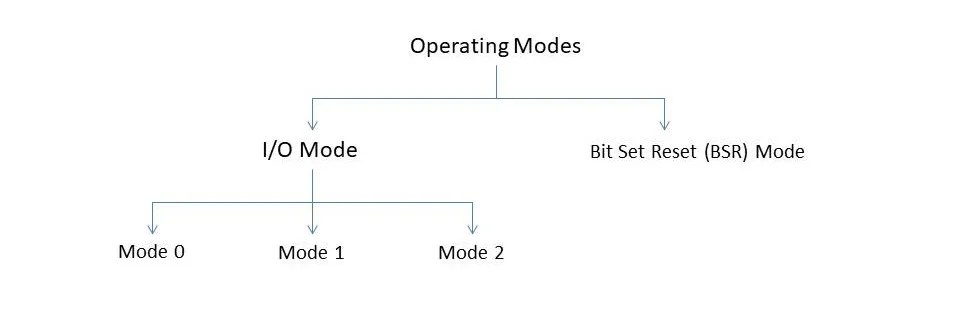
First, we will learn about the I/O mode (mode 0, mode 1, and mode 2), and then we will move on to BSR mode.
I/O mode
In I/O mode of operation, Ports A, B, and C of the 8255 can function in 3 different modes:
- Mode 0
- Mode 1
- Mode 2
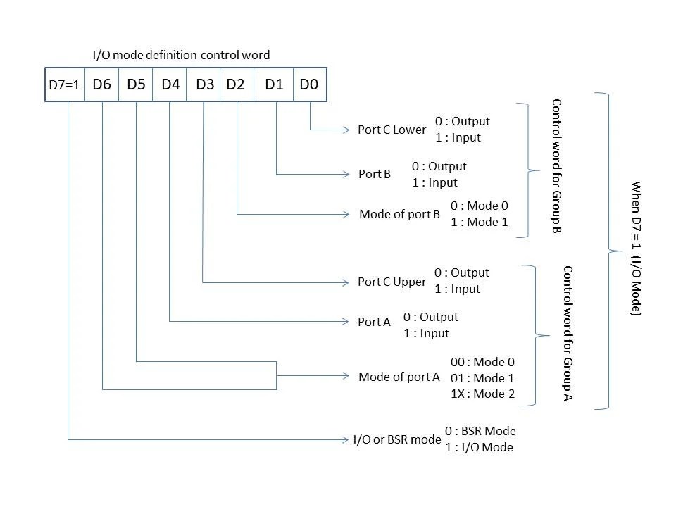
I/O mode control word
These modes can be selected by setting and resetting specific bits of the I/O mode control word.
You can observe from the illustration below how the microprocessor selects the mode of operation by issuing control instructions at the control port (control word).
In other words, the below diagram explains to you, “what exactly does the microprocessor write to the control port to set a particular port in a particular mode of operation.”
Let us learn about the mode 0 operation.
Mode 0
- This is the simplest mode of operation.
- In this mode, the I/O device cannot tell the microprocessor that it wants to read data or give data to the microprocessor. Hence, the microprocessor should know when to read and when to write data.
- The I/O device reads or writes data when it wants to.
- Similarly, the microprocessor reads or writes data according to the way we programmed it.
- There is no communication between the I/O device and the microprocessor.
From the above information, we can say that this mode is used for I/O devices whose timing characteristics are already known. For example, we can use this mode for an input device that wants to provide us with input every 0.5 seconds. So we program the microprocessor to read from that device after every 0.5 seconds without the input device actually telling the microprocessor that it wants to send data.
This mode can be applied when we need to read switch settings or temperature readings from a sensor. In such cases, the readings are always present at the input port. The microprocessor reads them when it requires the data for processing.
Mode 1 (Strobed I/O or Handshake I/O)
This mode uses handshaking to make the exchange of data more efficient. But what is handshaking?
In mode 1 and mode 2 operations of I/O ports, the I/O device and the processor can communicate with each other apart from the exchange of input and output data. It goes down like this:
When the input device writes data at a port, it tells the port that new data has entered. The port then informs the microprocessor that new unread data is there at the port. When the microprocessor is done reading the data, the port informs the input device that the data on the port is read and new data can be entered. This communication happens using the ‘handshaking signals’.
This above process is referred to as ‘handshaking.’ It is named so because it is similar to the handshaking between two strangers before they start talking to each other.
The lines of port C are used for handshaking signals. Thus, only port A and port B can work in mode 1, while port C provides handshake signals.
Three handshake signals are required for a port to work in handshake mode. Hence, port A and port B can both work in mode 1 simultaneously, with two lines of port C still remaining. The unused lines of port C for handshaking can be used for I/O in mode 0.
The below table specifies which lines of port C provide handshake signals for ports A and B.
| Mode of operation | Port | Input/Output | Lines of port C used for handshake |
| Mode 1 | Port A | Input | PC3, PC4, and PC5 |
| Mode 1 | Port A | Output | PC3, PC6, and PC7 |
| Mode 1 | Port B | Input and Output both | PC0, PC1, and PC2 |
One of the three handshake signals is ‘interrupt signal.’ This is an output signal from the 8255, which interrupts the microprocessor when required. 8255 provides additional functionality to enable or disable interrupts, depending on the requirement.
When interrupts are enabled, the I/O operations related to the 8255 are called ‘interrupt-driven I/O operations.’ And when the interrupts are disabled, they are referred to as ‘status check operations.’
This is because when interrupts are disabled, the microprocessor is not interrupted. It has to check if new data has arrived at the input buffer or new data is needed at the output buffer to initiate the read or write operation, respectively. Don’t worry about the technicality right now. Just focus on the fact that there are two ways of data transfer: ‘interrupt-driven’ and ‘status check transfer’ in the presence and absence of interrupts, respectively. So, the type of data transfer (explained in upcoming sections one by one) are:
- Interrupt driven input operation
- Interrupt driven output operation
- Status check input operation.
- Status check output operation
Enabling and disabling an interrupt
As you can observe in the block diagram below representing the simplified internal block structure, there are three EI (enable interrupt) flip flops marked with *. The value stored in these flip flops determines the enable status of the flip flops.

Now, it’s a little tricky here. Let us understand the process in steps.
- First, let us consider port B. When port B is programmed for mode 1 input or output, PC2 is reserved for one of the input handshake signals.
- In that case, we can enable the interrupt by setting the bit PC2 to 1 in BSR mode.
- If we manipulate PC2 in BSR mode while it is reserved for handshake signal (since port B is in mode 1), the value we set will be stored in port B EI flip flop, and it will not be reflected on the pin PC2.
- When port B is in mode 0, PC2 will work as normal I/O bit.
Similarly, when port A is programmed for mode 1 input operation, PC4 plays this role. To enable the interrupt, we set PC4 using BSR mode while port A is in mode 1 input. To disable it, we can reset the bit PC4. These value changes are not reflected on pin PC4 but are stored in port A input interrupt enable flip flop.
For port A programmed as output port in mode 1, PC6 plays this role.
Note: After the execution of mode definition control, port interrupts are already disabled. If we want an interrupt-driven data transfer, we need to enable them first.
Now, since you know that interrupts can be disabled, let us learn how data transfer takes place with and without interrupts.
Interrupt driven mode 1 input operation
We can program port A and port B to work in mode 1 independent of each other. In either case, there will be three handshake signals provided by the lines of port C.
- STB* (PC4 for port A and PC2 for port B)
It is an active low input signal for 8255. The input device gives a low going pulse at this pin whenever it has data to send to the microprocessor. When the pulse ends, i.e., when STB* goes from 0 to 1, the data provided by the input device is latched to the input buffer. It means that the input data is stored at the port for the microprocessor to pick up. - IBF (PC5 for port A and PC1 for port B)
This is an active-high output pin of 8255. It indicates the status of the input buffer, whether it is full or not. It goes high when there is data in the input buffer. It tells the microprocessor that “there is new data to be read at the input port” and also tells the input device that “there is unread data at the port and if you write new data, previous data may be lost.” It goes low when the microprocessor reads data from the input buffer. - INT (PC3 for port A and PC0 for port B)
This is also an active high output pin of 8255. Here, INT stands for interrupt. Whenever there is a pulse at STB* pin, there is some new data coming into the input buffer. When this pulse occurs, the INT signal goes high. This signal is connected to the interrupt pins of the microprocessor. It interrupts the microprocessor and urges it to read the new input data. When the microprocessor reads data, the RD* input signal of 8255 goes low, indicating read operation. When this read operation starts, INT goes low too as it has accomplished its purpose of interrupting the microprocessor and telling it to read the data.


Don’t be overwhelmed if the function of pins is still not clear. Let us now go through the process of data input from an input device. As we go through the process step by step, we will be referring to the timing diagram below.
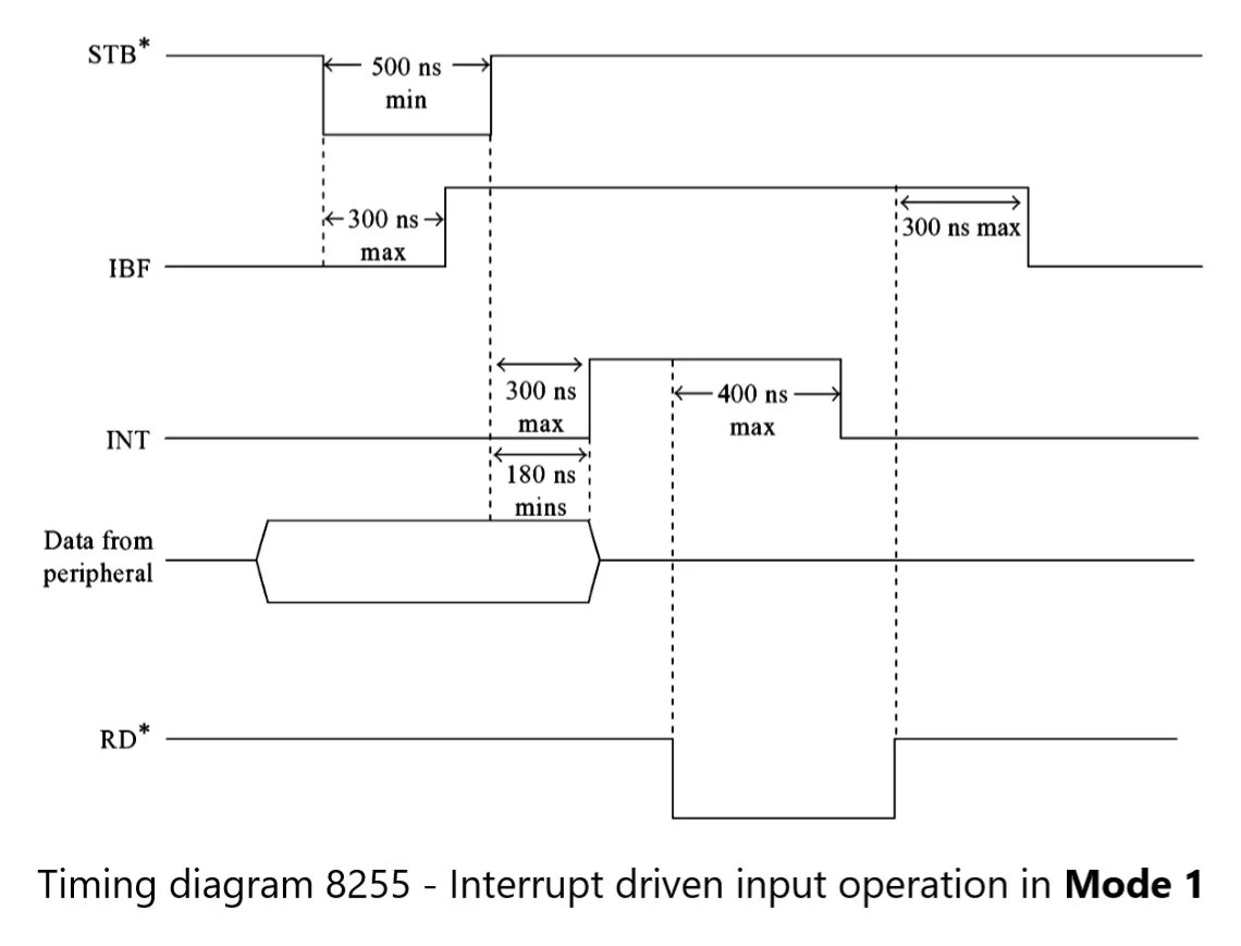
Step 1
Whenever there is new input data, there is a low going pulse on the active-low signal pin STB*, which exists for at least 500 ns. It indicates that there is new input data. Since there is new input data, the data is stored in the input buffer until it is read.
Step 2
To indicate that the input buffer is occupied by the unread input data, the IBF signal goes high. This happens after a maximum of 300 ns of starting of the pulse at STB*.
Step 3
During all this, the data from the peripheral is available at the input port. And it is supposed to be available for at least 180 ns after the end of the STB* pulse. It is shown in the timing diagram above.
Step 4
Within 300 ns of the ending of STB* pulse, the INT signal goes high, interrupting the microprocessor. The microprocessor should be programmed to read the data from the port using IN instruction on receiving this interrupt signal.
Step 5
As the microprocessor takes action (reads the data from the input port) when it is interrupted, the RD* signal goes low, indicating the read operation at the port.
Step 6
When 8255 gets RD* signal, it knows that data at the port is being read, and after the end of RD* signal within a maximum of 300 ns, the INT signal goes low too.
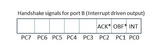
Interrupt driven mode 1 output operation
You have seen the details of the input operation in mode 1. Now, let us learn the handshaking process and details of interrupt-driven output operation in mode 1. The three handshaking signals are provided by the pins of port C are:
- ACK* (PC6 for port A and PC2 for port B)
This is an active low input signal for 8255. ACK stands for ‘acknowledge.’ When the output device wants data and reads data from a port, it sends a low going pulse at the ACK*. - OBF* (PC7 for pot A and PC1 for port B)
It is an active low output pin of 8255. When there is unread data in the output buffer, 8255 makes this signal low, and when the data present in the output buffer is read, this signal goes high. - INT (PC3 for pot A and PC0 for port B)
An active high output pin of 8255. 8255 interrupts the microprocessor using this signal to tell that the data at the output buffer has been read, and new data is required.

We will now go through the process of interrupt-driven output operation in mode 1 step by step, looking at the timing diagram as we proceed.

Step 1
When output devices want to read data, it reads from the output buffer and sends a low going pulse to the active low input pin ACK*, indicating that it has received the output data. This pulse is at least 300 ns in width.
Step 2
After a maximum of 350 ns from the start of the ACK* pulse, OBF* system goes from 0 to 1 (from active to inactive), indicating that the data in the buffer has been read and it no more contains new data.
To visualize properly, refer to the above timing diagram for every step.
Step 3
After a maximum of 350 ns from the end of the ACK* pulse, the INT signal goes high. By doing this, 8255 interrupts the microprocessor and tells it that “the data at the output buffer has been read and you need to write new data into it before the output device needs new data.
Step 4
After getting the interrupt signal from 8255, the microprocessor will take proper action (service the subroutine for that particular interrupt) and write data on the output port. The data will be stored in the output buffer. For writing this data, the input signal to 8255 WR* goes low, indicating that a write operation takes place.
Step 5
Now, since the write operation has taken place and the new data has not been read by the output device yet, there is no need for the INT signal to be high. So, the INT signal goes low after a maximum of 850 nanoseconds from the activation of WR* signal (or from the start of the WR* pulse, as you can observe from the timing diagram).
Step 6
Also, since there is unread data at the output buffer, the OBF* signal should also become 0. The OBF* signal goes from high to low after a maximum of 650 ns from the end of WR* pulse.
Status check input operation in mode 1
In this mode, the interrupt is disabled. Hence, the microprocessor won’t be interrupted by 8255. In order to determine if the data transfer is needed or not, we need the microprocessor to perform a status check.
This diagram shows the handshake signals provided by port C for a status check input operation for port A and port B, respectively.

Let us consider port B. Handshake signals are provided by PC2, PC1, and PC0.
- INTE (PC2 for port B and PC4 for port A)
This signal tells the EI status for port B, i.e., whether interrupt for port B is enabled or not. In this case, it must be low. - IBF (PC1 for port B and PC5 for port A)
This is an active-high output signal of 8255. It indicates whether the input buffer is filled with new data or not. IBF=1 means that the input buffer is full and IBF=0 means that the input buffer is empty. In order to know whether new data has arrived or not, the microprocessor should check the status of this signal. - INT (PC0 for port B and PC3 for port A)
This is the interrupt pin. But since interrupt is disabled, this signal always remains low in status check I/O operations.
Now, let’s go through the process of status check input operation at port B in mode 1.
When the input device wants to give input, it checks IBF. If IBF is low, indicating that the input buffer is empty, it gives a pulse at STB* and sends the input data. The new data is latched to the port buffer. Since there is unread data at the port buffer, the IBF signal goes high. Now, whenever the microprocessor reads IBF, the high value of IBF will signify that there is new data at the port, and the microprocessor will know that it needs to read the new input data. But since interrupt is disabled, INT always remains low in status check operations.
The status check output mode operation is quite similar.
Status check output operation in mode 1
It is almost similar to the status check input operation. But instead of the IBF signal, there is an active-low OBF*. Handshake signals are explained here.
This diagram shows the handshake signals provided by the port C for status check output operation for port A and port B, respectively.

- INTE (PC2 for port B and PC6 for port A)
This signal tells the EI status for port B, i.e., whether interrupt for port B is enabled or not. In this case, it must be low. - OBF* (PC1 for port B and PC7 for port A)
This is an active low output signal of 8255. It indicates whether the output buffer is filled with new data or not. OBF*=0 means that the output buffer is full and OBF*=1 means that the output buffer is empty. In order to know whether new data has arrived or not, the microprocessor should check the status of this signal. - INT (PC0 for port B and PC3 for port A)
This is the interrupt pin. But since interrupt is disabled, this signal always remains low in status check I/O operations.
When the output device wants to read data, it checks OBF*. If OBF* is low, indicating that the output buffer has new unread data, it gives a pulse at ACK* and reads the data from the output buffer. Since there is no unread data at the port buffer now, the OBF* signal goes high.
Now, whenever the microprocessor reads OBF*, the high value of OBF* will signify that there is no new data at the port, and the microprocessor will know that it needs to output new data. But since interrupt is disabled, INT always remains low during status check operations.
Mode 2 (Bidirectional I/O)
In mode 0 and mode 1, ports A and B can only work as either input ports or output ports. But in mode 2, port A can play both roles simultaneously. A port programmed in mode 2 can take inputs and give outputs. Since data transfer is bidirectional in mode 2, handshake signals required are also more.
There are five handshake signals required for port A to function in mode 1. These are provided by port C pins PC3-PC7. The remaining three pins can function as handshake pins for port B working in mode 1 or can function as normal I/O pins if port B is programmed to work in mode 0.
It can be easily deduced that only port A can work in mode 2 since only three pins of port C remain after allocating handshake signals to port A in mode 2 and the required number for port B also to work in mode 2 is five.
Port A : Mode 0, mode 1, mode 2
Port B : Mode 0, Mode 1
Port C : Mode 0
Recall the handshake signal allocations of port A in mode 1 input and output operations. In mode 2, the signal allocations and the meaning, significance, and functions of the signals remain the same. The following diagram will help you recall it.

Interrupt driven bidirectional operation
The handshake signals and their functions must be clear from the above diagram. Recall the details of the mode 1 input and output operations. In mode 2, the operations are quite similar. You can think of it as ‘both input operation and output operation from mode 1 are combined to form mode 2 operation’.
Visit the section on ‘Interrupt driven input operation in mode 1’ and read it once again. This time, read it while keeping only port A in mind. This is how the input operation takes place in mode 2.
Similarly, visit the section on ‘Interrupt driven output operation in mode 1’ and read that also once again, keeping port A in mind. This is how output operation takes place in mode 2.
You must have noticed that there are separate status pins IFB and OBF* and separate pins ACK* and STB for input and output. But there is just one single interrupt pin for both the operations. Thus, when the microprocessor is interrupted, it needs to check OBF* and IBF signals also to determine what kind of operation (input or output) is needed.
These operations are interrupt-driven. But interrupts can be disabled. In fact, initially interrupts are disabled, and we need to enable them. Enabling and disabling of the interrupts is discussed in the section on mode 1 operation under the heading ‘Enabling and disabling interrupts.’
Status check bidirectional operation
If we disable the interrupt, status I/O operations take place by checking the status signals OBF* and IBF. The interrupt signal always remains if disabled.
You can read the section ‘Status check input operation’ and ‘Status check output operation’ under the heading ‘Mode 1 (Strobed I/O or handshake I/O)’. Again, keep in mind port A while reading these sections. This is how status check bidirectional data transfer takes place.
BSR Mode (Control word)
As stated before, bits of port C can be set and reset individually in the BSR mode. It is achieved by writing the appropriate control instruction at the control port. These instructions are called ‘BSR mode control words.’ The illustration below explains what you need to write on the control port to manipulate the bits of port C in BSR mode.

That’s all for the 8255-Programmable Peripheral Interface. In our next post, we are going to explain the interfacing of 8255 with microprocessor 8085. We’ll also cover the interfacing of the 8255 with the 8051 in our free 8051 course.
We hope you understood the concepts underlined here. If you still have any doubts or follow-up questions, leave a comment below, and we will get in touch with you.