The MOSFET is the most commonly used compact transistor in digital and analog electronics. It has revolutionized electronics in the information age. In this article, we will see the basic principle of the working of MOSFETs and also look at a basic derivation for the IV characteristics of the NMOS transistor.
The flow of current is established in a MOSFET device due to the formation of an inverted charge layer. This inversion of charge is controlled by the controlling terminal called the “Gate terminal.” Thus, this controlling action of the current between two terminals called the “Drain,” and the “Source” by a third “Gate” terminal is what gives us the transistor action. We will see each concept in detail as we move forward.
Contents
Structure of MOSFET

There are four types of MOSFETs available, but for this article, we will focus mainly on only one of these four types. MOSFETs can be divided into two categories which are:
- Enhancement Mode MOSFET:
For this kind of MOSFET, there is no inversion layer present when we apply zero voltage at the gate terminal. On applying a gate voltage which surpasses a certain threshold voltage, we get an inversion in the bulk, and conduction between source and drain takes place. The structure for an enhancement-mode NMOS transistor (n-channel transistor) is shown in figure 1. - Depletion Mode MOSFET:
For a depletion-mode MOSFET, an inversion channel exists even when we apply zero voltage, as shown in figure 2. This is due to the fact that the threshold voltage of a MOS device with a p-type substrate can be negative, i.e., the electrons are already present when there is zero gate voltage.
For this article, we will only stick to Enhancement-mode MOSFET operations. The p-channel MOSFET structures are very similar. One will just have the source and drain of p-type semiconductors, and the substrate will be made of n-type.


The gate is a metal layer (in present-day CMOS technology, this is generally made up of polysilicon) shown by black color, which is deposited over an insulator. A layer of hatched lines shows the insulator (generally, this insulator is made up of Silicon-di-oxide). Some of the common notations used are 


Difference between PMOS and NMOS
From now, we will be mainly considering an n-channel enhancement type MOSFET by default until mentioned otherwise. But the derivation of I-V characteristics and the concepts regarding transistor action are very analogous for a p-type also. Thus, understanding the n-type MOSFET or NMOS will suffice.
Some differences between the PMOS and the NMOS transistor are shown below. Keeping these differences in mind will help in getting a better understanding of the analogy between NMOS and PMOS transistors.
| NMOS Transistor | PMOS Transistor |
| Source and Drain is made up of n-type semiconductor | Source and Drain is made up of p-type semiconductor |
| Substrate/Body is made up of p-type semiconductor | Substrate/Body is made up of n-type semiconductor |
| The majority carriers in the inversion channel are electrons(n-type) | The majority carriers in the inversion channel are holes(p-type) |
| The threshold voltage is a positive quantity | The threshold voltage is a negative quantity |
| Can be switched faster because the mobility of electrons is more than that of holes | Switching is slower because of holes being the majority carriers |
Biasing scheme for NMOS transistor
In this section, we will see a common biasing scheme for the NMOS. The biasing diagrams are shown in figure 3 and figure 4.
We’ll discuss “Body Effect” in the next article on non-ideal IV characteristics due to second-order effects.
For this simple biasing scheme, we have connected the Body terminal with the ground terminal. As shown in the diagrams, the source terminal is connected to the ground. We have connected a voltage source of 


Intuitive understanding of the IV characteristics
Before moving on to the mathematical derivation of the IV curves, there is some inherent understanding that can be achieved by observing the diagrams.
The threshold voltage
Different cases of biasing voltage
When 

When we have a 
The three modes of operation i.e., Cut-off, Triode (also referred to as linear region), and Saturation, will be discussed in detail once we start to derive the ideal IV characteristics properly.
Dependence of current on the voltages applied
By intuition, we can easily deduce that the current 

Mathematical derivation of ideal IV characteristics
In this section, we will solve some equations, which are an outcome from MOS capacitor physics and its operation in order to get the ideal IV characteristics of an NMOS device. The details regarding different modes of operation will also be discussed in this section.
Cut-Off Mode
In this mode of operation, the
Linear Mode (Triode Mode)

In figure 5, you can see the zoomed-in view of an NMOS transistor’s channel when it is conducting. We will first derive the IV relation for this configuration.
Suppose we take the voltage across the oxide layer at any point “x” distance away from the source terminal to be 
![[(V_{GS} - V_{T}) - V(x)]](https://s0.wp.com/latex.php?latex=%5B%28V_%7BGS%7D+-+V_%7BT%7D%29+-+V%28x%29%5D&bg=ffffff&fg=000&s=0&c=20201002)


The exact equation for charge per unit length in the inversion layer is given by :
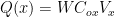 , replacing with
 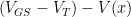 , we get:

Hence, at the source-edge, we have: 
We have velocity of electrons in the inversion layer given by:
 ;
;
Here 

And we also have: 
Current due to the majority charge carriers i.e. electrons in the inversion layer is given by:
current = 
(Note that the direction of current has already been considered in this equation, 
Hence, from these equations, we get a differential equation given as:
![-I_{D} = {-\mu_{n} \frac{dV}{dx}} \times W C_{ox} [(V_{GS} - V_{T}) - V(x)]](https://s0.wp.com/latex.php?latex=-I_%7BD%7D+%3D+%7B-%5Cmu_%7Bn%7D+%5Cfrac%7BdV%7D%7Bdx%7D%7D+%5Ctimes+W+C_%7Box%7D+%5B%28V_%7BGS%7D+-+V_%7BT%7D%29+-+V%28x%29%5D+&bg=ffffff&fg=000&s=0&c=20201002)
![I_{D} = \mu_{n} \frac{dV}{dx} W C_{ox} [(V_{GS} - V_{T}) - V(x)]](https://s0.wp.com/latex.php?latex=+I_%7BD%7D+%3D+%5Cmu_%7Bn%7D+%5Cfrac%7BdV%7D%7Bdx%7D+W+C_%7Box%7D+%5B%28V_%7BGS%7D+-+V_%7BT%7D%29+-+V%28x%29%5D+&bg=ffffff&fg=000&s=0&c=20201002)
![I_{D} dx = \mu_{n} W C_{ox} [(V_{GS} - V_{T}) - V(x)] dV(x)](https://s0.wp.com/latex.php?latex=+I_%7BD%7D+dx+%3D+%5Cmu_%7Bn%7D+W+C_%7Box%7D+%5B%28V_%7BGS%7D+-+V_%7BT%7D%29+-+V%28x%29%5D+dV%28x%29+&bg=ffffff&fg=000&s=0&c=20201002)
We integrate for both sides of the equation where x goes from 0 to L and V(X) goes from 0(at the source) to
![\int_{0}^{L} I_{D} dx = \int_{0}^{V_{DS}} \mu_{n} W C_{ox} [(V_{GS} - V_{T}) - V(x)] dV(x)](https://s0.wp.com/latex.php?latex=+%5Cint_%7B0%7D%5E%7BL%7D+I_%7BD%7D+dx%C2%A0+%3D+%5Cint_%7B0%7D%5E%7BV_%7BDS%7D%7D+%5Cmu_%7Bn%7D+W+C_%7Box%7D+%5B%28V_%7BGS%7D+-+V_%7BT%7D%29+-+V%28x%29%5D+dV%28x%29+&bg=ffffff&fg=000&s=0&c=20201002)
The current through the inversion channel is constant and hence
![I_{D} L = \mu_{n} W C_{ox} [(V_{GS} - V_{T}) V_{DS} - V^{2}_{DS}/2]](https://s0.wp.com/latex.php?latex=+I_%7BD%7D+L+%3D+%5Cmu_%7Bn%7D+W+C_%7Box%7D+%5B%28V_%7BGS%7D+-+V_%7BT%7D%29+V_%7BDS%7D+-+V%5E%7B2%7D_%7BDS%7D%2F2%5D+&bg=ffffff&fg=000&s=0&c=20201002) Therefore finally we get our drain current as a function of and to be:
Therefore finally we get our drain current as a function of and to be:
![I_{D} = \frac{\mu_{n} W C_{ox}}{2 L}[2 (V_{GS} - V_{T}) V_{DS} - V^{2}_{DS}]](https://s0.wp.com/latex.php?latex=I_%7BD%7D+%3D+%5Cfrac%7B%5Cmu_%7Bn%7D+W+C_%7Box%7D%7D%7B2+L%7D%5B2+%28V_%7BGS%7D+-+V_%7BT%7D%29+V_%7BDS%7D+-+V%5E%7B2%7D_%7BDS%7D%5D&bg=ffffff&fg=000&s=0&c=20201002)
Now, suppose we are operating at a point where our
![I_{D} = \frac{\mu_{n} W C_{ox}}{L} [ (V_{GS} - V_{T}) V_{DS}]](https://s0.wp.com/latex.php?latex=I_%7BD%7D+%3D+%5Cfrac%7B%5Cmu_%7Bn%7D+W+C_%7Box%7D%7D%7BL%7D+%5B+%28V_%7BGS%7D+-+V_%7BT%7D%29+V_%7BDS%7D%5D&bg=ffffff&fg=000&s=0&c=20201002)
Looking at the equation, we can see that if the drain-to-source voltage is much lower than the overdrive voltage, then the current varies linearly with the
Saturation Mode operation
The current

Thus after a certain point, we will see a phenomenon called “Pinch-Off”. This is shown in figure 6 where the inversion layer thickness goes to zero at the drain terminal edge. This means that the charge in the inversion layer at that point is zero. As we had the charge proportional to 


After this point,

Figure 7 shows the inversion layer of a transistor in saturation. We will derive the IV relation for the transistor in saturation by making some small changes in our original differential equation.
In the diagram, the point where the inversion charge becomes zero is given by x = L’. This means that at this point we have : V(x = L’) =
Thus, this time we will integrate from x=0 to x=L’ and our V(X) will rum from 0 (at source) to
![\int_{0}^{L'} I_{D} dx = \int_{0}^{V_{GS} - V_{T}} \mu_{n} W C_{ox} [(V_{GS} - V_{T}) - V(x)] dV(x)](https://s0.wp.com/latex.php?latex=%5Cint_%7B0%7D%5E%7BL%27%7D+I_%7BD%7D+dx%C2%A0+%3D+%5Cint_%7B0%7D%5E%7BV_%7BGS%7D+-+V_%7BT%7D%7D+%5Cmu_%7Bn%7D+W+C_%7Box%7D+%5B%28V_%7BGS%7D+-+V_%7BT%7D%29+-+V%28x%29%5D+dV%28x%29+&bg=ffffff&fg=000&s=0&c=20201002)
After solving and simplifying the equation, we get:
![I_{D} = \frac{\mu_{n} W C_{ox}}{2 L'} [(V_{GS} - V_{T})^2]](https://s0.wp.com/latex.php?latex=I_%7BD%7D+%3D+%5Cfrac%7B%5Cmu_%7Bn%7D+W+C_%7Box%7D%7D%7B2+L%27%7D+%5B%28V_%7BGS%7D+-+V_%7BT%7D%29%5E2%5D&bg=ffffff&fg=000&s=0&c=20201002)
For most of the practical cases, the actual channel length L’ is almost equal to L(original channel length of the MOSFET). The exact effect which changes the drain current due to variation in L’ is called “Channel Length Modulation”. This will be considered in the next article.
Plots showing the IV Characteristics
In this section, we will summarize the final equations we obtained for different regions of operation and see the corresponding ideal IV curves we get for an NMOS transistor.
Drain Current variation with Drain-to-Source Voltage
For the following plots, we have considered that 
- In Cut-Off Mode, the drain current
- In Linear Mode,
- In Saturation Mode,


The plots in figure 8 and figure 9 show the IV characteristics of the NMOS that we have considered in its linear mode of operation. The parabolic nature of the curve can be seen in figure 8. If we zoom-in the same plot near the origin, then we can see that the curves are almost linear which is the reason this region is named “Linear Region”.

In figure 10, the final IV characteristics of the NMOS is shown for different values of 
Drain Current variation with Gate-to-Source Voltage
Here we also consider a transistor for which


An analogy for Ideal IV characteristics of PMOS transistor
We will not be explicitly deriving the IV characteristics for the PMOS device separately because both the derivation and the final curves obtained are very similar to that of NMOS. A diagram showing the biasing scheme for a PMOS transistor is shown in figure 13.

It is observed from this diagram that the directions of the currents and voltages are inverted. For example, if we want to operate the PMOS in its saturation region, then we will apply a positive 

Conclusion
To conclude, in this article, we have considered the ideal IV characteristics of a MOSFET. We have seen the basic MOSFET structure, different types of MOSFETs, and some basic differences between them. Then we solved for the current and also plotted the current for different cases. But still, while deriving the current, we have assumed certain ideal scenarios. In the next article, we will see the non-idealities in the MOSFET and how it affects the IV characteristics of the MOSFET.
