Contents
What is Design for Testability, and why we need it?
Problems with manufacturing ICs
Today, semiconductors lie at the heart of ongoing advances across the electronics industry. The introduction of new technologies, especially nanometre technologies with 14 nm or smaller geometry, has allowed the semiconductor industry to keep pace with increased performance-capacity demands from consumers. This has brightened the prospects for future industry growth.
However, new technologies come with new challenges. Smaller die sizes increase the probability of some errors. Errors in ICs are highly undesirable. Here’s a list of some possible issues that arise while manufacturing chips.

- Density Issue: Fabrication processes have become quite complicated with the advent of deep-submicron design technologies. Design elements are coming closer and closer; they are becoming smaller and thinner. Billions of transistors are involved in present-day VLSI chips. So, the chances of two wires touching each other or a very thin wire breaking in between are high. These are a few sources of errors or faults. The point is, there can be many such errors that can creep in during the design and fabrication processes. So, with an increase in density, the probability of failure also becomes high.
- Software Issue: Moreover, apart from fabrication, there can even be errors in the translation process due to the bugs in CAD software tools used to design the chip.
- Application Issue: There are several critical applications, in which we can’t afford to have faults in the chip at any cost. For example, in medical or healthcare applications, a single fault in the equipment controllers may even risk the life of an individual. For rockets or space shuttles that run on cryogenic fuel, they may need their microcontroller or microprocessor to run on a broader temperature range. Hence the test conditions for these chips should be very application-specific and on an extreme level to prevent any future failures.
- Maintenance Issue: In case of any future failure, for repairing or maintenance, we need to identify the proper coordinates of fault. Since PCB sizes are also decreasing, multimeter testing isn’t a viable option anymore. Moreover, moving towards SoC (System on Chip) design, the modular design is losing its relevance, thereby making the maintenance process more expensive.
- Business Issue: If designed chips are found to be faulty, then it transforms into a substantial loss and penalty for the company. Later, we will discuss how detecting a fault earlier decreases the cost of doing business significantly.
The possibility of faults may arise even after fabrication during the packaging process.
With all these issues in mind, it becomes vital to test every chip before it can be shipped and in fact, test it after every level of manufacturing.
Solutions to these problems: DFT
Testing does not come for free. Modern microprocessors contain more than 1000 pins. They pack a myriad of functionalities inside them. If any single transistor inside a chip becomes faulty, then the whole chip needs to be discarded. We, consumers, do not expect faulty chips from manufacturers. But identifying that one single defective transistor out of billions is a headache. We may need to test every functionality with every possible combination. If testing is done that way, then the time-to-market would be so high that the chips may never reach the consumers. So, how do we tackle this? We use a methodology to add a feature to these chips. The methodology is called DFT; short for Design for Testability. And the feature it adds to a chip is ‘testability.’
In simple words, Design for testability is a design technique that makes testing a chip possible and cost-effective by adding additional circuitry to the chip.
Alternatively, Design-for-testability techniques improve the controllability and observability of internal nodes, so that embedded functions can be tested.
Role of DFT
Testing of Sequential Circuits
DFT offers a solution to the issue of testing sequential circuits. It’s kind of hard to test sequential circuits. Since there are clocks involved along with the flip-flops.
Unlike combinational circuits, we can’t determine the output of sequential circuits by merely looking into the inputs. Sequential circuits consist of finite states by virtue of flip-flops. The output also depends upon the state of the machine. It is difficult to control and observe the internal flip-flops externally.
Hence, the state machines cannot be tested unless they are initialized to a known value. And to initialize them, we need a specific set of features in addition to the typical circuitry. DFT enables us to add this functionality to a sequential circuit and thus allows us to test it.
Improving the chip manufacturing process
DFT accomplishes two significant goals in the chip manufacturing process:
- Reject Defective Modules (Product Quality)
Testing checks the errors in the manufacturing process that are creating faults in the chips being designed. If faults can be detected earlier, then the underlying process causing the faults can be discarded at that point. This saves time and money as the faulty chips can be discarded even before they are manufactured.
- Monitor and Improve Manufacturing Process
Testing is applied at every phase or level of abstraction from RTL to ASIC flow. This identifies the stage when the process variables move outside acceptable values. This simplifies failure analysis by identifying the probable defect location. Meticulous monitoring improves process-line accuracy and decreases the fault occurrence probability.
Can DFT permanently eliminate faults?
So, does testing guarantee that the chip will never be faulty again?
No, faults can arise even after the chip is in consumer’s hands. A chip may misbehave anytime if it is exposed to a very high temperature or humid environment or due to aging.
Want a live explanation? If you have an unlocked processor, you can try to overclock your CPU using this tutorial. But would you do it? Please don’t!
Overclocking is a method to increase the system frequency and voltage above the rated value. An improperly configured overclocking can mess up with timing metrics and cause instability. Prolonged overclocking would overheat and stress out your system to shorten the lifespan of your computer. This may cause intermittent faults in the chip and random crashes in the future. Adding to this, it may void your warranty too. This example is just one high-level explanation of how a fault may occur in real life.
Verification vs Testing
What is the difference between Verification and Testing?
Verification proves the correctness and logical functionality of the design pre-fabrication. The process is done after the RTL (Register Transfer Logic) design is coded with hardware description languages like VHDL or Verilog. It is done using a testbench in a high-level language. This is performed only once before the actual manufacturing of chip. In industry, this is done using formal verification processes like UVM (Universal Verification Methodology) using System Verilog. Verification is a vast topic on its own and we will cover it in this VLSI track and link it here soon.
In contrast, testing tries to guarantee the correctness of the manufactured chips at every abstraction level of the chip design process. Testing needs to be performed on each manufactured chip because each one of them has an equal probability of being faulty during the fabrication or packaging process. By doing testing, we are improving the quality of the devices that are being sold in the market.
| Verification | Testing |
| Verifies correctness of the design. | Verifies correctness of the manufactured hardware. |
| Performed by simulation, hardware emulation, or formal methods. | Two-part process:
|
| Performed once prior to manufacturing.
|
Test application is performed on every manufactured device. |
| Responsible for the quality of design.
|
Responsible for the quality of devices.
|
Career choice: Verification vs DFT
Let’s segue into the career aspect of these two stages for a moment.

Some Terminologies
Here are a few terminologies which we will often use in this free Design for Testability course. Don’t fret if you can’t completely understand them yet, we will be covering them in-depth in this course.
Testing: An experiment in which the system is put to work and its resulting response is analyzed to ascertain whether it behaved correctly.
Diagnosis: Process for locating the cause of misbehavior in the circuit if it happened.
Defect: Refers to a flaw in the actual hardware or electronic system.
Fault: It is a model or representation of defect for analyzing in a computer program.
Error: It is caused by a defect and happens when a fault in hardware causes line/ gate output to have a wrong value.
Failure: This occurs when a defect causes misbehavior in the circuit or functionality of a system and cannot be reversed or recovered.
Fault Coverage: Percentage of the total number of logical faults that can be tested using a given test set T.
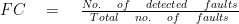
Defect Level: Refers to the fraction of shipped parts that are defective. Or, the proportion of the faulty chip in which fault isn’t detected and has been classified as good.

where Y is the yield, means the fraction of the chips fabricated that are good.
Levels of Testing
Testing is carried out at various levels:
- Chip-level, when chips are manufactured.
- Board-level, when chips are integrated on the boards.
- System-level, when several boards are assembled together.
There is an empirical rule of thumb that it is ten times more expensive to test a device as we move to the next higher level (chip → board → system). As we move to higher levels, more components are integrated, which makes the fault detection and localization much more difficult and expensive.
Sources of Faults in ICs
Here are a few possible sources of faults:
- In the fabrication process like missing contact windows, parasitic transistors, etc.
- Defects in the materials like cracks or imperfections in the substrate, surface impurities, etc.
- Aging caused by Dielectric breakdown, electron migration, etc.
- During packaging like Contact degradation, disconnection, etc.
Classification of Faults
Faults can be classified into various subcategories.
DFT Techniques
DFT techniques are broadly classified into two types:
Ad-hoc techniques
These are a collection of techniques or set of rules (do’s and don’ts) in the chip design process learned from design experience to make design testability more comfortable to accomplish. Basically, these are the rules that have been gathered over time after experiencing various errors.
- Test vector generation is simplified
- Very easy to implement, no design rule or constraints and area overhead is very less.
- Are not always reusable, since each design has its specific requirements and testability problems.
- It doesn’t guarantee high testability levels regardless of the circuit.
- Not systematic enough to enable a uniform approach to testable circuit design.
Following are a few ad-hoc set of rules that designers generally follow:
- Large circuits should be partitioned into smaller sub-circuits to reduce test cost.
- Test access points must be inserted to enhance the controllability & observability of the circuit. This is done either by increasing the number of nodes or by multiplexing existing primary outputs for the internal nodes to be observed.
Structured techniques
In this technique, extra logic and signals are added to the circuit to allow the test according to some predefined procedure.
In contrast to Ad-hoc, structured DFT implies that the same design approach can always be used and assure good testability levels, regardless of the circuit function. This technique is the only solution to modern world DFT problems.
There is, however, a price to pay, which usually consists of accepting that some design rules (rather a design style) are enforced and that additional silicon area and propagation delays are tolerated.
Following are a few examples of structured DFT which we will cover extensively in future lessons:
- Scan Path
- Partial Scan
- Level Sensitive Scan
- BIST
- Boundary Scan
Summary (TL;DR)
This was a short introduction to the concept of Design for Testability in VLSI. We also saw an overview of what it entails and what’s to come in this course. The key takeaway is just that there is a lot of room for error in the manufacturing of ICs. These errors can be costly in more ways than just financially. To reduce these errors significantly, a methodology known as DFT exists. This methodology adds a bunch of features to test the chips. To learn how that’s done, and everything it entails, keep up with the course!
